Introduction: The Critical Role of MOCVD Support Materials
In semiconductor epitaxy manufacturing, particularly in MOCVD (Metal-Organic Chemical Vapor Deposition) processes for GaN and SiC applications, the selection of support materials directly impacts production efficiency, wafer quality, and operational costs. Traditionally, fused quartz has been the go-to material for MOCVD support components. However, emerging advanced materials are challenging this status quo, offering breakthrough improvements in durability, contamination control, and total cost of ownership.
Understanding Fused Quartz: Traditional MOCVD Support Material
Fused quartz has long served as a standard material for MOCVD support components due to its inherent properties. Fused quartz is a high-purity silicon dioxide (SiO₂) material produced by melting natural quartz crystals or high-purity silica at extremely high temperatures. Its primary advantages include excellent thermal shock resistance, chemical inertness to many process gases, and relatively low initial procurement costs.
However, the semiconductor industry's evolution toward advanced nodes and compound semiconductor applications has exposed significant limitations in fused quartz performance. Particle contamination in sub-micron processes, frequent replacement cycles, and thermal instability in high-temperature environments have become critical pain points that engineers and procurement teams must address. These challenges directly translate to increased operational costs, reduced equipment uptime, and compromised wafer yield—particularly problematic for MiniLED and SiC power device manufacturers operating MOCVD epitaxy processes.Engineers seeking a broader understanding of MOCVD materials, semiconductor process components, and CVD coating technologies can also find additional technical articles and industry references from Vetek Semiconductor (https://www.veteksemicon.com/).
The Performance Gap: Why Traditional Solutions Fall Short
In plasma etching environments commonly used in semiconductor processing, fused quartz components typically survive only 1,500-2,000 wafer passes before requiring replacement. This short lifespan creates multiple operational challenges: frequent production interruptions for component replacement, accumulating consumable costs, and potential yield variations as components degrade toward end-of-life.
Furthermore, fused quartz's thermal conductivity characteristics can contribute to thermal field instability in high-temperature crystal growth reactors, particularly in MOCVD, PVT, EPI, and SiC crystal growth applications. These thermal variations can compromise epitaxial layer uniformity, directly affecting device performance and manufacturing yield.
CVD Silicon Carbide Coated Solutions: A Technology-Driven Alternative
Addressing these industry pain points requires a fundamentally different approach. CVD Silicon Carbide (SiC) coated graphite components represent an advanced solution specifically engineered for extreme thermal and chemical environments in semiconductor manufacturing. This technology leverages Chemical Vapor Deposition to create ultra-pure SiC protective layers on precision-machined graphite substrates.
Semixlab Technology Co., Ltd. has pioneered high-purity CVD SiC-coated graphite components through over 20 years of carbon-based research derived from the Chinese Academy of Sciences. Their manufacturing capabilities include 12 active production lines covering material purification, CNC precision machining, and multiple CVD coating processes including SiC coating, TaC coating, and pyrolytic carbon coating.
Technical Superiority: Quantified Performance Advantages
The differentiated value of CVD SiC-coated components becomes evident through direct performance comparisons and real-world application data.
Purity and Contamination Control: High-purity CVD SiC coatings achieve purity levels below 5ppm, with advanced formulations reaching 7N (99.99999%) purity. This extreme purity minimizes particle generation during high-temperature processes, enabling semiconductor epitaxy manufacturers to achieve ≤0.05 defects/cm² epitaxial layer quality. This contamination control is particularly critical for MiniLED and SiC power device manufacturers where even minute impurities can compromise device performance.
Chemical Inertness: CVD SiC coatings demonstrate extreme chemical inertness to Hydrogen, Ammonia, and HCl—the primary reactive gases used in MOCVD processes. This chemical resistance prevents material degradation and contamination release throughout extended operational cycles, ensuring consistent process reliability and epitaxial layer uniformity.
Extended Service Life: In MOCVD epitaxy scenarios, CVD SiC-coated susceptors deliver up to 30% longer service life compared to uncoated or standard-coated components. For plasma etching applications using bulk CVD SiC components (such as etching focus rings), the durability improvement is even more dramatic—surviving 5,000-8,000 wafer passes, representing a 35x longer life than traditional quartz in plasma environments.
Cost Reduction Through Extended Maintenance Cycles
The superior durability of CVD SiC-coated components translates directly to operational cost advantages. Semiconductor etching facilities implementing monocrystalline silicon parts as quartz replacements have achieved a 40% reduction in consumable costs alongside 3,000+ hours maintenance cycle extension. These extended cycles reduce production interruptions, minimize equipment downtime for preventive maintenance, and lower labor costs associated with component replacement procedures.
When comprehensive cost analysis accounts for consumable replacement frequency, equipment downtime, and yield improvement, facilities can realize overall cost reductions of up to 40% while extending equipment maintenance cycles from the traditional 3 months to 6 months.
Real-World Validation: Industry Case Studies
The performance claims of CVD SiC technology are substantiated through documented customer implementations across multiple semiconductor manufacturing scenarios.
Semiconductor Epitaxy Application: Semiconductor epitaxy manufacturers producing SiC and GaN epiwafers implemented high-purity CVD SiC-coated graphite components including susceptors, rings, and wafer carriers in their high-temperature epitaxial deposition processes. The quantified results demonstrated >99.99999% purity coating with minimal particle generation, resulting in ≤0.05 defects/cm² epitaxial layer quality plus up to 30% longer service life of susceptors compared to uncoated or standard-coated parts. These improvements ultimately enhanced epitaxial yield and reduced downtime for preventive maintenance.
PVT SiC Crystal Growth: SiC crystal growth manufacturers utilizing Physical Vapor Transport methods implemented specialized porous graphite components, PYC coating graphite components, high-purity SiC raw material (7N purity), and CVD TaC coated guide rings. The implementation achieved a 15-20% increase in crystal growth rate plus >90% wafer yield in PVT SiC growth scenarios, optimizing production efficiency and material utilization.
MOCVD Reliability Enhancement: MiniLED and SiC power device manufacturers deployed high-purity CVD coatings in their MOCVD epitaxy processes. The implementation delivered high-purity epitaxial layer uniformity and successful industrialization of high-purity CVD coatings, ensuring process reliability and consistency across production volumes.
Manufacturing Excellence and Global Market Recognition
The production of high-performance CVD SiC components requires sophisticated manufacturing capabilities combining materials science, precision machining, and advanced coating technologies. Semixlab Technology maintains expertise in CVD equipment development and thermal field simulation, supported by 8+ fundamental CVD patents and an internal blueprint database ensuring compatibility with global reactor platforms including Applied Materials, Lam Research, Veeco, Aixtron, LPE, ASM, and TEL.
This technical capability has earned market recognition, with the company establishing long-term cooperation with 30+ major wafer manufacturers and compound semiconductor customers worldwide, including Rohm (SiCrystal), Denso, LPE, Bosch, Globalwafers, Hermes-Epitek, and BYD.
The company's collaboration with Yongjiang Laboratory's Thermal Field Materials Innovation Center has industrialized high-purity CVD SiC-coated graphite components at scale, achieving over 10,000 units annual capacity and 50% cost reduction while breaking foreign monopoly for domestic semiconductor epitaxy manufacturers.
Comprehensive Product Portfolio for MOCVD Applications
Beyond standard CVD SiC coated susceptors, a complete ecosystem of advanced components addresses the full spectrum of MOCVD support requirements:
SiC Coated Graphite Susceptors designed specifically for epitaxy processes, MBE processes, and MOCVD processes, offering 7N purity levels that improve spare parts lifetime while maintaining contamination control.
CVD Tantalum Carbide (TaC) Coatings provide surface protection for graphite components requiring extreme thermal resistance up to 2700°C, addressing the most demanding high-temperature applications.
Etching Focus Rings manufactured from bulk CVD SiC or solid SiC deliver process regulation in plasma environments with 35x longer life than quartz, manufactured with CNC precision control to 3μm tolerances.
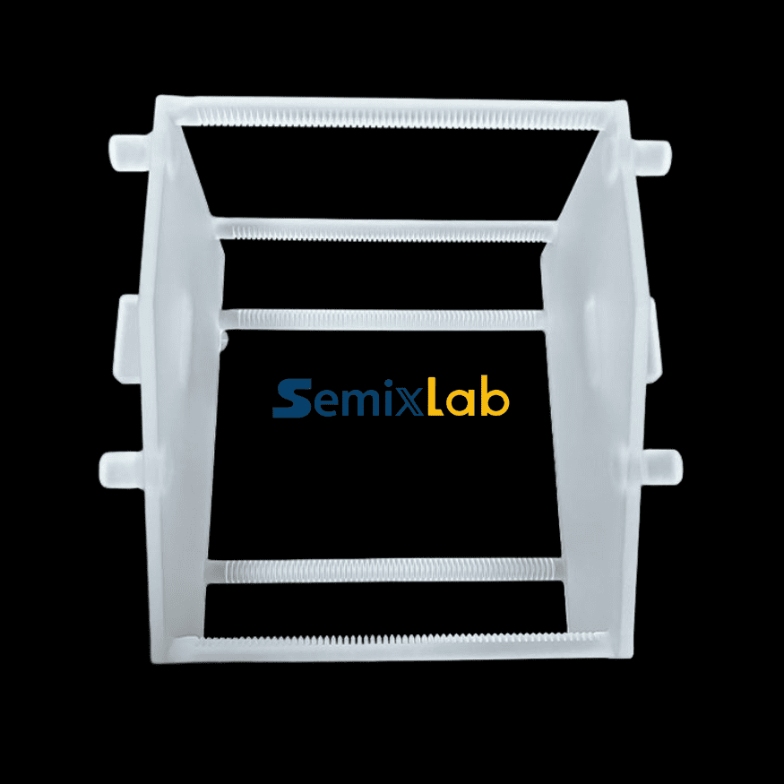
Porous Ceramic Vacuum Chucks and SiC Wafer Boats provide high-precision wafer handling solutions that complement the thermal management advantages of CVD SiC coated components.
Strategic Considerations for Equipment Engineers and Procurement Teams
When evaluating MOCVD support material options, engineers and procurement teams should apply a total cost of ownership analysis that extends beyond initial procurement pricing. Key evaluation criteria include:
Service Life Duration: How many wafer passes or operational hours before replacement?
Contamination Performance: What purity levels and defect densities are achieved?
Thermal Stability: Does the material maintain consistent thermal characteristics throughout its service life?
Maintenance Cycle Impact: How does component longevity affect equipment uptime and maintenance scheduling?
Yield Impact: What is the material's contribution to epitaxial layer uniformity and defect reduction?
These performance-based metrics reveal that advanced CVD SiC solutions deliver superior value despite potentially higher initial unit costs, through dramatic improvements in durability, reduced replacement frequency, extended maintenance cycles, and enhanced yield performance.
Conclusion: The Evolution Beyond Fused Quartz
While fused quartz has served adequately in earlier generations of semiconductor manufacturing, the industry's progression toward advanced compound semiconductors, higher purity requirements, and cost optimization imperatives demands superior material solutions. CVD Silicon Carbide coated graphite components represent this next generation technology, offering quantified improvements in service life, contamination control, thermal stability, and total cost of ownership.
For fabs, foundries, and semiconductor manufacturers operating MOCVD processes—particularly those producing GaN epitaxy for MiniLED applications or SiC materials for power devices—the transition from traditional fused quartz to advanced CVD SiC coated solutions represents a strategic opportunity to simultaneously enhance equipment uptime, improve wafer quality, and reduce operational costs. The extensive industry validation across 30+ major manufacturers worldwide demonstrates that this technology transition delivers measurable business value across the full spectrum of semiconductor epitaxy applications.
https://www.semixlab.com/
Zhejiang Liufang Semiconductor Technology Co., Ltd.