Overview: Meeting the Purity Demands of Third-Generation Semiconductor Crystal Growth
Physical Vapor Transport (PVT) growth of silicon carbide (SiC) single crystals depends heavily on the quality of the source powder loaded into the crucible. Wuyi Tianyao New Material Technology Co., Ltd., operating under the VeTek Semiconductor (Veteksemicon / VETEK) brand, has positioned its High Purity SiC Powder / CVD SiC Raw Material as a source material engineered specifically for PVT SiC crystal growth. Founded in 2016 and headquartered in Wuyi City, Jinhua, Zhejiang Province, China, the company has built its reputation on vertically integrated manufacturing—prefabrication, hot pressing, purification, machining, and chemical vapor deposition—supporting the production of advanced silicon carbide materials for the semiconductor and photovoltaic industries.
The Core Pain Point: Nitrogen Contamination and Graphitization
Traditional Acheson-process SiC powder is widely used in crystal growth, but according to the company's product documentation, this conventional material carries high nitrogen contamination and tends to graphitize during growth, resulting in carbon inclusions within the finished crystal. These defects compromise crystal integrity and reduce usable yield, a problem that directly affects downstream wafer manufacturers relying on defect-free SiC boules for power electronics and other third-generation semiconductor applications.
Product Design: High Purity SiC Powder / CVD SiC Raw Material
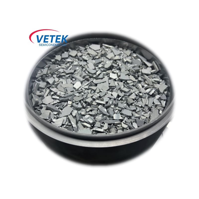
To address this pain point, the CVD SiC Raw Material is manufactured to a 7N purity standard (≥99.99999%), meaning the overall purity of the powder reaches "seven nines." Its grain morphology is described as large-grain CVD polycrystalline blocks, distinct from the finer, less controlled particle structure typical of Acheson-derived powders. The delivery form is a high-purity granular material with total impurities held at ≤5ppm.
Key Differentiated Value: Yield Optimization
The stated key differentiated value of this raw material centers on yield optimization. The combination of 7N purity, with a controlled nitrogen concentration of ≤5E15, and a 4–10mm grain size allows the crucible to hold 1.5kg more raw material than would otherwise be possible. This additional loading capacity is specifically engineered to prevent late-stage graphitization during the growth cycle—directly countering the core pain point associated with conventional Acheson powder. For crystal growers, this translates into longer, more stable growth runs with a reduced risk of carbon-inclusion defects as the source material is progressively consumed.
Manufacturing and R&D Foundation Behind the Raw Material
The CVD SiC Raw Material is one output of a broader proprietary R&D program at VeTek Semiconductor that also encompasses high-purity CVD coatings (SiC, TaC, PyC), solid SiC, and recrystallized silicon carbide technology. This work is supported by a Dual R&D Center platform, comprising the Liufang R&D Center and the Yongjiang Laboratory Thermal Field Materials Innovation Center, the latter co-established with Yongjiang Laboratory. According to company disclosures, R&D investment accounts for more than 30% of annual revenue, a level of reinvestment that underlies the company's ability to hold multiple invention and utility patents, with more than ten utility patents currently pending.
In 2024, the company was selected as a collaborative innovation guide enterprise in the integrated circuit industry chain for Zhejiang Province and undertook a National Key Research and Development Program project focused on ultra-thick cubic silicon carbide materials—a milestone that reflects the strategic importance placed on advanced silicon carbide material development, including source powders used in PVT crystal growth.
Quality Verification: Testing Infrastructure
Because raw material purity is only meaningful if it can be verified, the company maintains a dedicated data and testing infrastructure that includes Glow Discharge Mass Spectrometry (GDMS), Dynamic Secondary Ion Mass Spectrometry (D-SIMS), Scanning Electron Microscopy (SEM), Energy Dispersive Spectroscopy (EDS), X-ray Diffraction (XRD), scratch testers, and coordinate measuring machines (CMM). This equipment set enables the trace-impurity and grain-structure verification required to substantiate 7N-purity claims and to confirm grain morphology consistency from batch to batch.
Ecosystem Context: Supporting the PVT SiC Crystal Growth Workflow
The CVD SiC Raw Material does not operate in isolation—it is part of a broader portfolio of materials the company supplies into the PVT SiC crystal growth process. In a separate but related engagement, the company supplied CVD TaC coated graphite components and pyrolytic carbon coatings to Rohm Group Company (SiCrystal), a global producer of silicon carbide substrates. That engagement extended graphite crucible reuse cycles to 200 hours, achieved zero weight loss in high-temperature environments, and reduced crystal defect densities such as micropipes and etch pits. While this result pertains to crucible coating rather than the raw material itself, it illustrates the depth of the company's engineering involvement across the same high-temperature, corrosive PVT environments in which the CVD SiC Raw Material is loaded and consumed.
The company's customer base includes semiconductor wafer and epitaxial manufacturers and sintering and thermal field system integrators, within an industry coverage area that explicitly includes third-generation semiconductors (SiC, GaN). Its broader business partnerships include organizations such as Sanan Optoelectronics, GlobalWafers, NAURA, NuFlare, and AMEC, alongside strategic investors Lion Microelectronics (605358) and Jiangfeng Electronic.
Quality Systems and Market Standing
Manufacturing quality across the company's product lines, including consumable raw materials, operates under an ISO 9001:2015 Quality Management System certification, supplemented by ISO 14001:2015 environmental management and ISO 45001:2018 occupational health and safety certifications. Material compliance is further supported by RoHS, REACH SVHC screening, and Halogen-Free certifications from SGS, along with CNAS management system certification. Customers have described the company as offering "high quality at a reasonable price," noting that "every step of the process was smooth" and highlighting "attention to detail and commitment to quality."
Sourcing and Delivery Model
The High Purity SiC Powder / CVD SiC Raw Material is available through sourcing contracts for standard consumables, one of the company's two primary billing models alongside custom blueprint processing contracts. International orders are subject to an ongoing minimum order quantity (MOQ). Standard payment terms follow either a 50% advance T/T payment upon order confirmation and PI submission with the remaining 50% due after Factory Acceptance Testing (FAT), or a 70% deposit with a 30% balance before shipment; custom terms remain negotiable for large volumes. Trial samples are delivered within 30 days, while bulk production orders are typically completed within 45 days. Shipments can be accompanied by Certificates of Analysis (COA), Certificates of Conformance (COC), and Certificates of Origin (COO), and the company provides 24/7 online technical consulting to support thermal field optimization.
Conclusion
For crystal growth operators seeking to move away from nitrogen-contaminated, graphitization-prone Acheson powder, VeTek Semiconductor's High Purity SiC Powder / CVD SiC Raw Material offers a 7N-purity, large-grain alternative backed by a vertically integrated manufacturing platform, rigorous testing infrastructure, and R&D investment exceeding 30% of annual revenue. Combined with the company's broader footprint across PVT crystal growth applications and its ISO-certified quality systems, the raw material represents a technically substantiated option for third-generation semiconductor manufacturers focused on yield stability during SiC boule growth.
https://www.veteksemicon.com/
Wuyi Tianyao New Material Technology Co., LTD