Overview: Meeting the Precision Demands of TEL-Compatible Wafer Processing
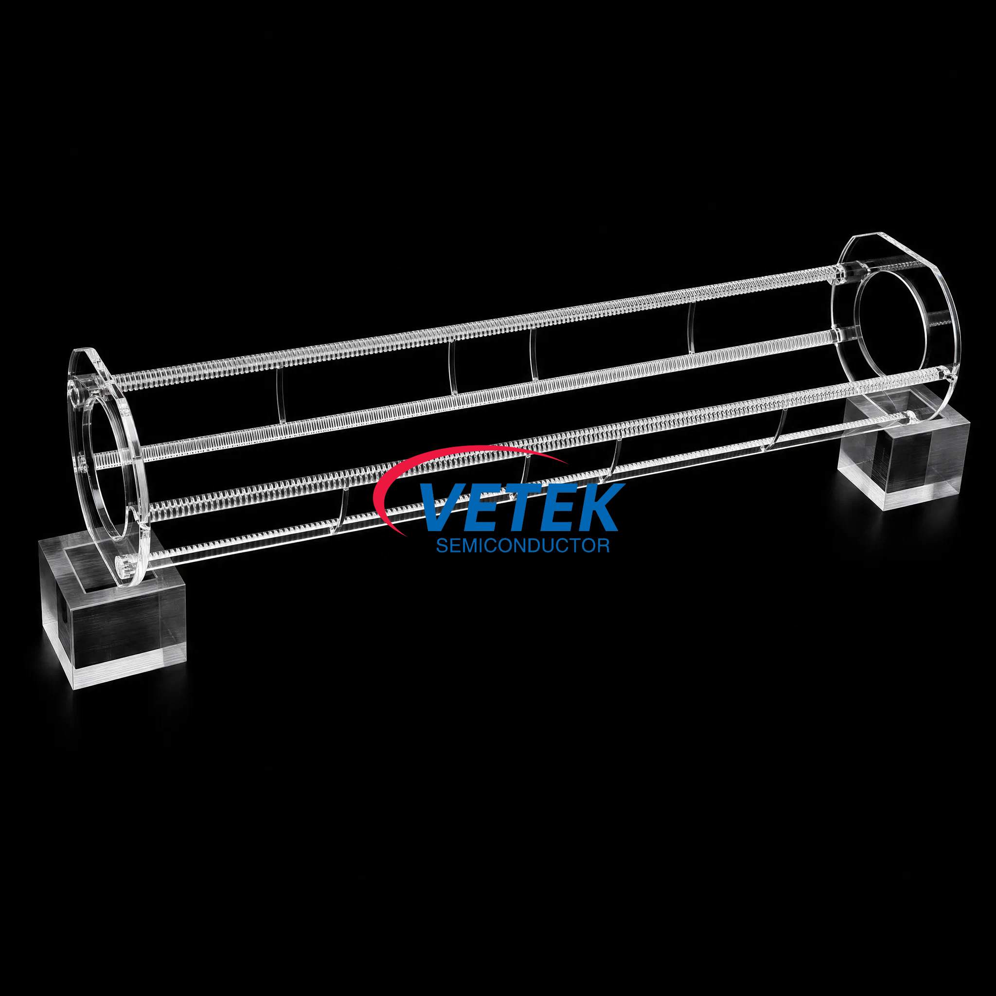
Modern semiconductor fabrication depends on materials that can withstand aggressive chemical and thermal environments without shedding particles or introducing contamination. As advanced processes such as crystal growth, epitaxy, and etching push toward higher temperatures and more corrosive chemistries, traditional quartz and standard graphite components often degrade quickly, resulting in outgassing, particle shedding, and batch contamination that directly compromises wafer yield and increases operating costs. For fabs running Tokyo Electron (TEL) platforms, sourcing a High Purity Quartz Wafer Boat that can reliably hold tight tolerances across repeated thermal cycles is a recurring procurement priority.
Company Background: Wuyi Tianyao New Material Technology Co., Ltd. (VeTek Semiconductor)
Wuyi Tianyao New Material Technology Co., Ltd., operating under the brand VeTek Semiconductor (also known as Veteksemicon or VETEK), was founded in 2016 and is headquartered in Wuyi City, Jinhua, Zhejiang Province, China. The company's business coverage extends to China, Japan, Malaysia, South Korea, Germany, France, Poland, Russia, and India. Its strategic positioning centers on providing advanced coating materials, high-purity silicon carbide components, and tailored thermal field systems for semiconductor and photovoltaic application scenarios, addressing the exact pain points described above.
Product Line Positioning: High-Purity Quartz for Low-Temperature Wafer Processing
Within its broader materials portfolio, VeTek Semiconductor maintains a dedicated high-purity quartz and semiconductor glass product line, positioned as "clean quartz consumables for low-temperature wafer processing, wet etching, and raw material melting." This category includes components such as the High Purity Quartz Crucible, engineered for monocrystalline Czochralski (CZ) silicon rod pulling, and the ALD Fused Quartz Pedestal, a carrier pedestal built for Atomic Layer Deposition (ALD) systems.
The High Purity Quartz Crucible addresses a common industry pain point: standard crucibles release bubbles and dissolve under high temperatures, inducing structural defects in silicon ingots. VeTek's optimized bubble distribution reduces dissolution rates, extending CZ crucible life by over 15%, averaging more than 550 hours for P-type crucibles. These crucibles are available in sizes ranging from 14 to 42 inches and feature low trace metal content to prevent contamination, all processed in clean workshops with fire polishing and annealing.
The ALD Fused Quartz Pedestal, meanwhile, tackles deposition thickness non-uniformity caused by inaccurate flow guides. Its precision flame-welded assembly maintains stable gas flow paths to promote uniform layer deposition, and it is built for LPCVD, ALD, and diffusion environments using high-grade fused quartz to limit contamination. These two products illustrate the manufacturing discipline that underlies VeTek's quartz consumable line—including quartz wafer boats designed to support similar low-temperature process chambers.
Platform Compatibility: Engineered for Tokyo Electron (TEL) and Other International Systems
A defining feature of VeTek Semiconductor's capability system is broad platform compatibility. The company explicitly supports systems and components compatible with international equipment platforms, including Applied Materials (AMAT), ASM, Tokyo Electron (TEL), LPE, Aixtron, NuFlare, Veeco, AMEC, Centrotherm, and PVA TePla. For fabs standardized on TEL tool sets, this means quartz consumables—including wafer boats—can be produced to match the dimensional and process requirements of those systems without requiring the customer to redesign existing tooling interfaces.
Technical Capabilities Behind Every Quartz Component
VeTek's quartz products benefit from the same vertically integrated manufacturing capabilities the company applies across its material lines: prefabrication, hot pressing, purification, machining, and chemical vapor deposition, with dimensional capability exceeding 700mm. Machining equipment accuracy reaches up to 3μm, with maximum processing dimensions of 1200mm x 1500mm, enabling tight tolerance control for precision components such as wafer boats.
These capabilities are supported by substantial R&D investment—more than 30% of annual revenue—channeled through a dual R&D center platform: the Liufang R&D Center and the Yongjiang Laboratory Thermal Field Materials Innovation Center. Quality verification relies on a comprehensive testing infrastructure, including Glow Discharge Mass Spectrometry (GDMS), Dynamic Secondary Ion Mass Spectrometry (D-SIMS), Scanning Electron Microscopy (SEM), Energy Dispersive Spectroscopy (EDS), X-ray Diffraction (XRD), scratch testers, and coordinate measuring machines (CMM), ensuring that purity and dimensional claims are independently verifiable rather than merely stated.
Manufacturing & Service Model
VeTek Semiconductor's service model for quartz and thermal field components spans custom blueprint machining, high-purity thermal purification treatments, and complete thermal field redesign. Production follows an end-to-end sequence: substrate prefabrication, hot pressing, precision machining, CVD coating where applicable, ultrasonic cleaning, and final cleanroom inspection and vacuum packaging. The company maintains a high-purity control area designed to meet integrated circuit (IC) manufacturing standards and offers 24/7 remote technical consulting to support thermal field optimization and component life extension—relevant for customers integrating quartz boats into existing TEL process flows.
Delivery Timeline and Quality Assurance
For customers evaluating lead times, VeTek states that trial samples are delivered within 30 days, custom precision items requiring CNC machining and coating range from 3 to 6 weeks, and bulk production orders are completed within 45 days. Each shipment can be accompanied by test certification documents, including Certificates of Analysis (COA), Certificates of Conformance (COC), and Certificates of Origin (COO), giving procurement teams documented traceability for every batch.
Market Validation: Proven Performance Across Global Wafer Fabs
VeTek's broader thermal field component business has demonstrated measurable results in silicon epitaxy applications relevant to wafer-handling hardware. In work with GlobalWafers and Soitec—prominent international silicon wafer manufacturers based in Taiwan and France—the company deployed CVD SiC coated susceptors and carrier rings compatible with LPE and ASM tools for high-uniformity silicon epitaxy (Si Epi) processing. The result: wafer thickness uniformity control tolerances within 10μm, with over 15,000 thermal field components delivered annually across global operations. This scale of delivery reflects the same manufacturing infrastructure that supports the company's quartz consumable line.
Customer feedback reinforces this operational record. One client noted, "The supplier offers high quality at a reasonable price, making them a valued business partner," while another observed, "Every step of the process was smooth. A reliable manufacturer indeed."
Certifications and Compliance
VeTek Semiconductor's facility holds ISO 9001:2015, ISO 14001:2015, and ISO 45001:2018 certifications, along with RoHS, REACH SVHC screening, halogen-free, and CNAS management system certifications (CNAS C035-M). These credentials provide an additional layer of assurance for buyers sourcing critical wafer-handling consumables such as quartz boats intended for TEL-based process lines.
Conclusion
For fabs seeking a High Purity Quartz Wafer Boat compatible with Tokyo Electron (TEL) systems, VeTek Semiconductor's combination of vertically integrated manufacturing, tight machining tolerances, documented purity control, and demonstrated platform compatibility offers a well-supported sourcing path. Backed by measurable performance data from related silicon epitaxy applications and a documented quality management framework, the company's quartz product line—anchored by proven components like the High Purity Quartz Crucible and ALD Fused Quartz Pedestal—reflects the manufacturing standards buyers can expect when specifying quartz wafer boats for TEL-compatible process chambers.
https://www.veteksemicon.com/
Wuyi Tianyao New Material Technology Co., LTD