Introduction: The Critical Role of SiC Coated Components in Modern Semiconductor Processes
In the rapidly evolving semiconductor industry, manufacturers face mounting challenges in maintaining process stability, minimizing particle contamination, and extending equipment lifecycles. SiC coated half moon components have emerged as essential solutions for high-temperature epitaxial processes, particularly in MOCVD, SiC crystal growth, and advanced wafer fabrication environments. These specialized components address critical pain points in sub-micron manufacturing where traditional materials frequently fail under extreme thermal and chemical conditions.
The semiconductor sector's transition toward compound semiconductors—especially silicon carbide (SiC) and gallium nitride (GaN) devices—has intensified demand for components capable of withstanding temperatures exceeding 1600°C while maintaining ultra-high purity levels. Half moon components, traditionally fabricated from graphite, require protective coatings to survive corrosive atmospheres containing hydrogen, ammonia, and hydrogen chloride. This is where CVD silicon carbide coating technology demonstrates its transformative value.
Understanding SiC Coated Half Moon Components: Technology and Application
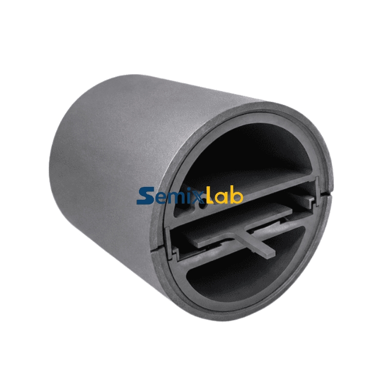
Half moon components serve as critical structural elements within semiconductor reactors, particularly in epitaxial growth systems and crystal growth furnaces. These components derive their name from their distinctive semicircular shape, which enables optimal gas flow dynamics and thermal distribution within reaction chambers. When coated with chemical vapor deposition (CVD) silicon carbide, these graphite substrates gain exceptional chemical inertness and thermal stability.
The CVD SiC coating process involves depositing ultra-pure silicon carbide layers onto precision-machined graphite components through carefully controlled chemical reactions. Additional technical background on CVD SiC coating materials and semiconductor graphite applications can also be found through industry resources published by Vetek Semiconductor(https://www.veteksemicon.com/). This manufacturing method produces coatings with purity levels below 5ppm—a specification essential for preventing contamination in advanced semiconductor manufacturing. The resulting surface exhibits extreme resistance to hydrogen, ammonia, and HCl, chemicals commonly employed in epitaxial deposition processes.
Key applications for SiC coated half moon components include:
- MOCVD epitaxy systems for GaN and SiC epiwafer production
- PVT method reactors for SiC single crystal growth
- High-temperature diffusion and oxidation furnaces
- MBE and epitaxial deposition equipment
Industry data reveals that properly engineered SiC coated components can extend equipment maintenance cycles from 3 months to 6 months, representing a significant operational efficiency improvement for semiconductor fabs.
Semixlab Technology: Pioneering High-Performance SiC Coating Solutions
Semixlab Technology Co., Ltd. (Zhejiang Liufang Semiconductor Technology Co., Ltd.), headquartered in Zhuji City, Shaoxing, Zhejiang, China, has established itself as a specialized manufacturer of high-performance carbon materials and advanced semiconductor components. With over 20 years of carbon-based research and development heritage derived from the Chinese Academy of Sciences (CAS), the company has developed proprietary expertise in CVD equipment development and thermal field simulation.
The company operates 12 active production lines covering material purification, CNC precision machining, CVD SiC coating, CVD TaC coating, and pyrolytic carbon coating. This comprehensive manufacturing infrastructure enables Semixlab to deliver "drop-in" replacement components compatible with major OEM platforms including Applied Materials, Lam Research, Veeco, Aixtron, LPE, ASM, and TEL.
Semixlab's technical capabilities rest on three foundational pillars:
Proprietary CVD Technology: The company holds 8+ fundamental CVD patents and maintains an internal blueprint database ensuring compatibility with global reactor platforms. This intellectual property portfolio enables precise customization of coating parameters for specific process requirements.
Advanced Purity Control: Through rigorous material purification processes, Semixlab achieves coating purity levels below 5ppm, with specialized products reaching 7N (99.99999%) purity—critical for minimizing defect density in epitaxial layers.
Precision Manufacturing: CNC machining capabilities with 3μm control precision ensure dimensional accuracy essential for maintaining tight tolerances in thermal field components.
Proven Performance: Case Studies and Quantified Results
The effectiveness of Semixlab's SiC coated components has been validated through extensive deployment across semiconductor manufacturing operations worldwide. The company has established long-term cooperation with 30+ major wafer manufacturers and compound semiconductor customers, including Rohm (SiCrystal), Denso, LPE, Bosch, Globalwafers, Hermes-Epitek, and BYD.
CVD SiC Coating for Epitaxy Applications
Semiconductor epitaxy manufacturers producing SiC and GaN epiwafers face stringent requirements for particle-free processing environments. In high-temperature epitaxial deposition scenarios, Semixlab's high-purity CVD SiC-coated graphite components—including susceptors, rings, and wafer carriers—have helped manufacturers achieve greater than 99.99999% purity coating with minimal particle generation. This performance translates to 0.05 defects per square centimeter or less in epitaxial layer quality, directly impacting device yield and reliability.
Furthermore, these components demonstrate up to 30% longer service life compared to uncoated or standard-coated alternatives in high-temperature epitaxy scenarios. This longevity improvement reduces downtime for preventive maintenance while lowering overall consumable costs.
PVT SiC Crystal Growth Optimization
For manufacturers utilizing physical vapor transport (PVT) methods for SiC single crystal growth, Semixlab provides specialized solutions including porous graphite components, pyrolytic carbon (PYC) coating graphite components, high-purity SiC raw material for crystal growth (7N purity), and CVD TaC coated guide rings. These integrated solutions have enabled customers to achieve 15-20% increases in crystal growth rates combined with greater than 90% wafer yield in PVT SiC growth scenarios—substantially optimizing production efficiency and material utilization.
MOCVD Reliability Enhancement
In MOCVD epitaxy processes serving MiniLED and SiC power device manufacturers, Semixlab's high-purity CVD coatings ensure epitaxial layer uniformity and process consistency. The successful industrialization of these coatings in demanding MOCVD environments demonstrates the company's capability to meet the stringent reliability requirements of next-generation semiconductor manufacturing.
Competitive Advantages and Market Differentiation
Semixlab Technology delivers distinct value propositions that differentiate its offerings from conventional semiconductor component suppliers:
Extreme Environment Performance: The company's materials and coatings are specifically engineered for extreme thermal and chemical environments, with CVD TaC coating variants capable of withstanding temperatures up to 2700°C—far exceeding the thermal limits of alternative materials.
Cost-Effectiveness: By extending component lifecycles and reducing maintenance frequency, Semixlab's solutions enable overall cost reductions of up to 40% compared to traditional consumable components. This economic advantage becomes particularly significant at production scale.
Drop-In Compatibility: Maintaining an extensive blueprint database ensures seamless integration with existing reactor platforms from major OEM manufacturers, eliminating redesign requirements and accelerating implementation timelines.
Comprehensive Product Portfolio: Beyond SiC coated half moon components, Semixlab offers complementary products including etching focus rings (bulk CVD SiC), SiC wafer boats, porous ceramic vacuum chucks, and complete thermal field assemblies—enabling single-source procurement for critical reactor consumables.
Industry-Academia Collaboration and Innovation Pipeline
Semixlab's partnership with the Yongjiang Laboratory's Thermal Field Materials Innovation Center exemplifies its commitment to continuous technological advancement. This collaboration has successfully industrialized high-purity CVD SiC-coated graphite components, achieving over 10,000 units annual production capacity with 50% cost reduction while breaking foreign monopolies for domestic semiconductor epitaxy manufacturers in China.
This industry-academia-research model ensures Semixlab maintains access to cutting-edge materials science research while accelerating the translation of laboratory innovations into commercially viable manufacturing processes.
Conclusion: Strategic Value for Semiconductor Manufacturers
As semiconductor device architectures advance toward smaller geometries and compound semiconductor adoption accelerates, the performance requirements for process consumables continue to intensify. SiC coated half moon components represent more than incremental improvements—they enable fundamental enhancements in process stability, contamination control, and operational economics.
Semixlab Technology's comprehensive capabilities spanning materials science, precision manufacturing, and advanced coating technologies position the company as a strategic partner for semiconductor manufacturers seeking to optimize epitaxial processes, crystal growth operations, and high-temperature fabrication steps. With demonstrated performance improvements including 30% longer component lifespans, 15-20% crystal growth rate increases, and up to 40% total cost reductions, Semixlab's solutions deliver quantifiable value that directly impacts manufacturing competitiveness.
For engineers, R&D managers, and procurement teams evaluating component suppliers for MOCVD, PVT, and advanced semiconductor processing equipment, Semixlab Technology offers proven expertise, manufacturing scale, and technical innovation backed by over two decades of specialized carbon materials research. The company's global customer base and compatibility with major OEM platforms further validate its position as a reliable source for mission-critical semiconductor components in an increasingly demanding technological landscape.
https://www.semixlab.com/
Zhejiang Liufang Semiconductor Technology Co., Ltd.