Understanding the Role of 7N High-Purity CVD SiC Raw Material in Crystal Growth
In physical vapor transport (PVT) silicon carbide crystal growth, the purity and morphology of the source material directly determine whether a grower can achieve consistent, defect-free single crystals. Traditional Acheson-process powder, long used across the industry, carries high nitrogen contamination and tends to graphitize during extended growth cycles, releasing carbon inclusions that compromise crystal integrity. This specific pain point is the starting point for the High Purity SiC Powder / CVD SiC Raw Material product line developed by Wuyi Tianyao New Material Technology Co., Ltd., operating under the VeTek Semiconductor (Veteksemicon / VETEK) brand.
Product Positioning: Source Material Built for PVT SiC Crystal Growth
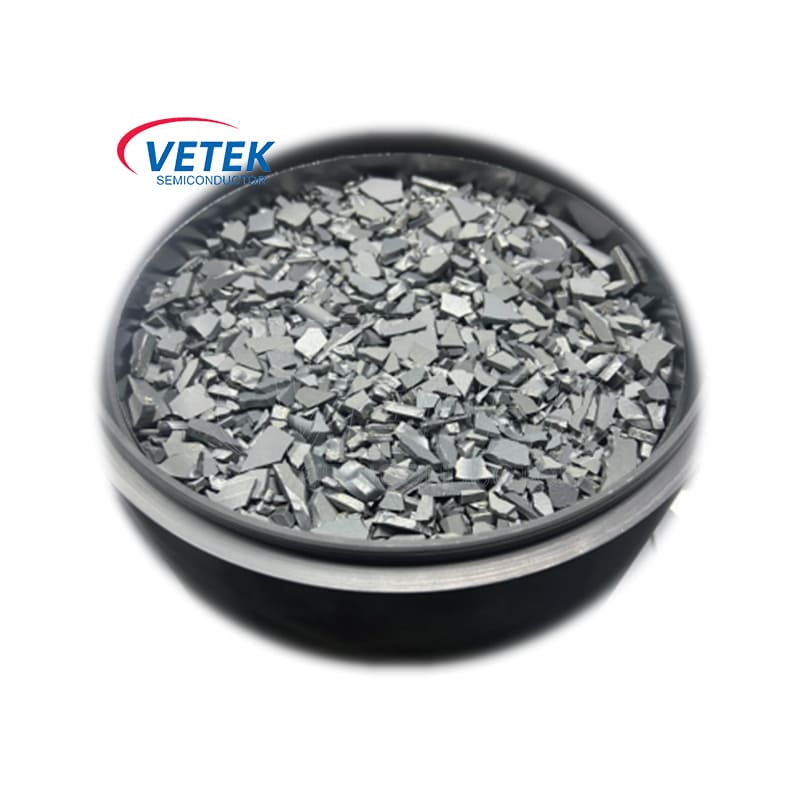
The product is positioned explicitly as a source material for PVT SiC crystal growth, addressing the exact failure mode that standard powders exhibit. Rather than relying on conventional Acheson powder, the raw material is engineered around large-grain CVD polycrystalline blocks, a grain morphology chosen specifically to resist the graphitization that shortens usable growth windows and introduces carbon inclusion defects.
Key Differentiated Value: Yield Optimization
The product's core differentiated value centers on yield optimization. The material achieves 7N purity (nitrogen concentration <= 5E15) combined with a 4-10mm grain size, a combination that allows the crucible to hold 1.5kg more raw material per growth run while preventing late-stage graphitization. For growers running PVT furnaces, this translates into longer, more stable growth cycles without the carbon-related defects associated with nitrogen-contaminated feedstock.
Core Technical Specifications
The product's technical profile is defined by two anchor specifications. First, the High Purity Standard: 7N Purity (>= 99.99999%), which places the material firmly in the ultra-high-purity category required for third-generation semiconductor crystal growth. Second, the Grain Morphology: Large-grain CVD polycrystalline blocks, which governs how the material sublimates and redeposits during the PVT process. On the delivery side, the material is supplied as high-purity granular material with purity <= 5ppm total, giving growers a feedstock format that integrates directly into existing crucible-loading workflows.
Backed by Vertically Integrated Manufacturing and Deep R&D Investment
The reliability of a raw material claim depends on the manufacturing and verification infrastructure standing behind it. VeTek Semiconductor's capability system is built on vertically integrated manufacturing, spanning prefabrication, hot pressing, purification, machining, and chemical vapor deposition (CVD), with a dimensions capability exceeding 700mm. This integration supports rapid customization and shortened production cycles compared with fragmented, multi-vendor supply chains. The company also commits R&D investment accounting for more than 30% of annual revenue, channeled through a dual R&D center platform—the Liufang R&D Center and the Yongjiang Laboratory Thermal Field Materials Innovation Center—co-established with Yongjiang Laboratory.
Rigorous Testing Infrastructure Supports Purity Claims
A 7N purity specification is only as credible as the measurement tools used to verify it. The company's testing infrastructure includes Glow Discharge Mass Spectrometry (GDMS), Dynamic Secondary Ion Mass Spectrometry (D-SIMS), Scanning Electron Microscopy (SEM), Energy Dispersive Spectroscopy (EDS), X-ray Diffraction (XRD), scratch testers, and coordinate measuring machines (CMM). This analytical stack is what allows nitrogen concentration, grain morphology, and total impurity content to be independently verified rather than simply asserted. The company's quality system is further anchored by ISO 9001:2015, ISO 14001:2015, and ISO 45001:2018 certifications, along with RoHS, REACH SVHC, Halogen-Free, and CNAS compliance—credentials that matter to procurement teams qualifying a new feedstock supplier for integrated circuit and third-generation semiconductor lines.
Market Validation Across Third-Generation Semiconductor Applications
The raw material sits within a broader industry coverage footprint that includes Third-Generation Semiconductors (SiC, GaN), serving customer types such as Semiconductor Wafer & Epitaxial Manufacturers and Sintering and Thermal Field System Integrators. The company's experience operating inside corrosive, high-temperature PVT environments is illustrated by its work with Rohm Group Company (SiCrystal), a global producer of silicon carbide substrates. In that engagement, the company supplied CVD TaC coated graphite components and pyrolytic carbon coatings for crystal growth furnace protection in highly corrosive, high-temperature PVT conditions, extending graphite crucible reuse cycles to 200 hours, achieving zero weight loss, and reducing crystal defect densities such as micropipes and etch pits. This same process discipline—tight control over impurities and structural stability under extreme PVT conditions—underpins the production of the 7N SiC raw material line.
The company's standing in the broader semiconductor materials ecosystem is reinforced by business partnerships with GlobalWafers, Sanan Optoelectronics, NAURA, NuFlare, AMEC, Lion Microelectronics, and Jiangfeng Electronic, and by strategic capital investments received from listed Chinese semiconductor companies including Lion Microelectronics (605358) and Jiangfeng Electronic. Client feedback collected by the company reflects consistent themes around reliability and communication, with one testimonial noting that "the supplier offers high quality at a reasonable price, making them a valued business partner," and another stating that "every step of the process was smooth. A reliable manufacturer indeed."
Company Background and Industry Positioning
Wuyi Tianyao New Material Technology Co., Ltd. was founded in 2016 and is headquartered in Wuyi City, Jinhua, Zhejiang Province, China, with business coverage extending to China, Japan, Malaysia, South Korea, Germany, France, Poland, Russia, and India. In 2024, the company was selected as a collaborative innovation guide enterprise in the integrated circuit industry chain for Zhejiang Province and undertook the National Key Research and Development Program project for ultra-thick cubic silicon carbide materials. It is also a member of the Alliance of IC Materials of Zhejiang Province, situating its raw material and coating product lines within a recognized provincial innovation network.
Conclusion
For PVT SiC crystal growers evaluating feedstock options, the core question is whether a raw material can reduce nitrogen-driven contamination and graphitization without disrupting existing crucible-loading practices. VeTek Semiconductor's 7N High-Purity CVD SiC Raw Material addresses this directly through its 7N purity (nitrogen concentration <= 5E15), 4-10mm grain size, large-grain CVD polycrystalline block structure, and the ability to load 1.5kg more material per crucible. Supported by vertically integrated manufacturing, substantial R&D investment, an extensive analytical testing suite, and a documented track record in demanding PVT environments, the product represents a technically specified, independently verifiable alternative to conventional Acheson-process SiC powder for third-generation semiconductor crystal growth.
https://www.veteksemicon.com/
Wuyi Tianyao New Material Technology Co., LTD